Understand and improve EMC of PCB
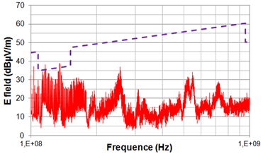
Electromagnetic compatibility (EMC) is a major concern for electronic equipments, which is still not perfectly understood by designers. Electromagnetic emission and immunity issues need to be thoroughly understood by professionals to successfully design their printed circuit boards (PCB). A careful placement and routing of PCB can improve significantly EMC. However, applying the adequate guideline requires a good understanding of electromagnetic issues associated to PCB. Otherwise, the modification applied at PCB level may be inefficient. This training is dedicated to technicians, engineers, researchers involved in electronic design who want to clarify the origin of EMC issues at PCB level and learn the techniques to fix them. No prerequisites in EMC are required. Only basic knowledges about electronic, PCB design and manufacturing are necessary. The objective of this training is twofold: The concepts presented during the courses will be illustrated through hardware and software demos with IC-EMC.
- Clarify EMC issues at PCB level, demystify the electromagnetic concepts related to these issues, understand their effect on electronic equipments, propose simple tools to evaluate EMC performances of PCB
- Present the main placement and routing techniques to improve EMC of PCB, learn how to analyze and manage EMC at PCB level, validate these techniques on real case studies
Program:
Day 1: Basis
Basic concepts for EMC at PCB level:Tools to identify EMC issues at PCB level:
- Introduction, context, EMC purpose
- Spectral contents of signal
- Stray impedance of components
- Transmission line
- Common-mode vs. differential-mode
- Radiation
- Ground
- Determining current return path
- Basis about spectrum analyzer
- Current probe
- Estimation of radiation from common-mode current measurement
- Near-field probe
- Estimation of PCB trace radiation from magnetic field measurement
- Low-cost VNA
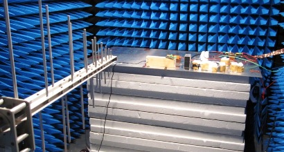
- Visit of an EMC lab
Day 2 - EMC rules for PCB design - part 1
EMC design rules for signal integrity:EMC design rules for power integrity:
- Frequency condition
- Impedance control of PCB lines (single-ended and differential lines)
- Routing of PCB traces
- Effects of via and stub
- Control of reference plane
- Effect of symmetry on differential lines
- Crosstalk
- Case study
EMC design rules to reduce radiated emission:
- Power distribution network of PCB
- Role of parasitic inductance
- Simple model to analyse PI problem
- Power-ground plane pairs
- General strategy to ensure power integrity
- Decoupling budget - Single-point methodology
- Placement of decoupling capacitors
Case study 1: Improve EMC of a digital board
- Identification of parasitic antenna at PCB level
- Reduce loop radiation
- Shielding of sensitive traces
- Board edge radiation
- Effect of split planes
- Radiation from cables
- Placement of connectors
Day 3 - EMC rules for PCB design - part 2
EMC design rules to reduce conducted emission:Case study 2: Improve EMC of a DC-DC converter EMC design rules for mixed-signal board:
- Real performances of EMC filter
- EMC filter placement
- Transient suppressor placement
- Case study: EMC filter
- EMC design rules for DC-DC converter
Case study 3: Improve EMC of a mixed-signal board Conclusion:
- Reference separation
- Partitioning
- Split planes
- Image plane violation
- Bridging
- Isolation with a common ground plane
- Placement of mixed-signal circuits
- Design methodology
- Advanced tools for EMC of PCB
Registration:
Formation continue INSA de ToulouseContact:
Email: Alexander.boyer <at> insa-toulouse.fr
Update: November 24, 2017


