Advanced Tools in IC-EMC
[S] and [Z] paralemeters for N port devices |
Conversion from S to Z parameters and import of measurements
in Touchstone format. Comparisons between measurements and simulations. |
Automatic susceptibility extraction |
Extraction of susceptibility threshold
of ICs to 1MHz-5GHz radiofrequency disturbances, with control of susceptibility criterion, power and frequency. |
XML near field scan support |
Interface for importing XML near-field scan measurement data according to the IEC 61 967 XML standard |
Automatic TLine generation |
Analytical
formulas to extract electrical parameters of different kind of transmission
lines and interconnects |
3D reconstruction from IBIS |
Build the 3D aspect of the package, locate I/Os and evaluate the whole package R,L,C |
3D package model using PEEC |
Construction of a 3D view of the IC package and 3D extraction of R, L, C
of each pins from partial elements computations based on quasi-static approximation. |
Time-Domain-Reflectometry |
Simulation of voltage
waveform, forward voltage, reflected voltage, impedance, reflection coefficient
profiles vs time |
S-Parameter de-embedding |
Imports Touchstone
S parameter measurement file and deembeds the measurements. |
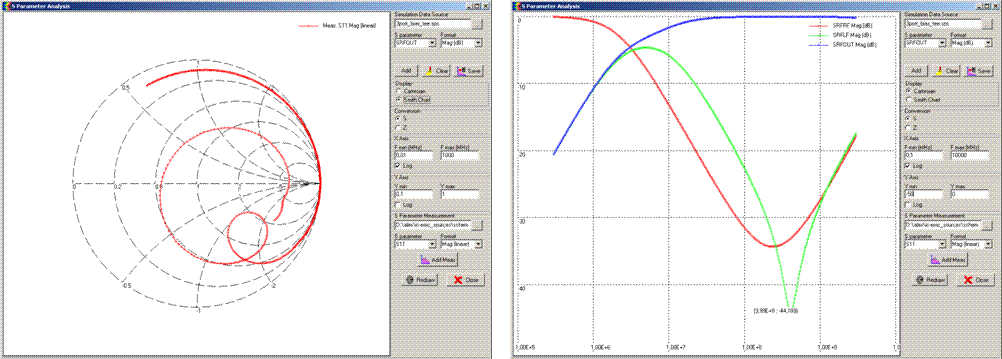
S and Z parameters simulation for N port
devices
IC-EMC proposes S parameters simulation on N port devices.
A special screen allows conversion from S to Z parameters and import of measurements
in Touchstone format. Comparisons between measurements and simulations help
users to build equivalent models of N port devices (circuit, PCB, cable...). Following
figures presents various S parameter measurement and simulation results.
[Top]
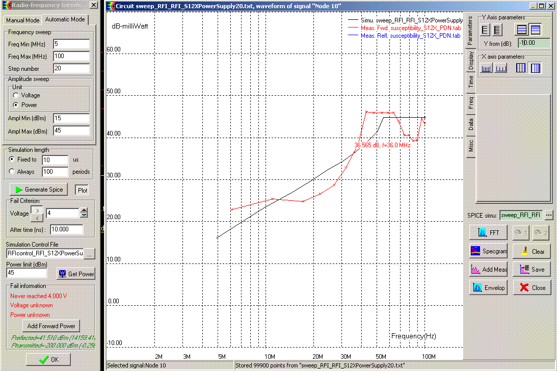
Automatic extraction of IC susceptibility
threshold to harmonic disturbances
IC-EMC offers a tool dedicated to extraction of susceptibility threshold
of circuits to radiofrequency disturbances, in relation with industrial standards
of EMC of ICs (IEC 62132). Susceptibility of circuits is extracted through
WinSPICE transient simulation. IC-EMC controls the frequency sweep of RF disturbances,
helps the user to define a particular immunity criterion and extract the required
forward, reflected and transmitted power to make the circuit fail. The figure
below describes the user control interface for susceptibility simulation (on
the left) and the Power vs Frequency plane where simulated and measured susceptibility
threshold are compared.
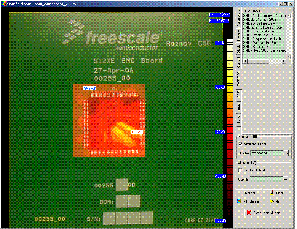
Near field scan data in XML format import
Near field scan measurements and simulations produce a large amount of data
ot be processed. The format of the data is closely linked to the supplier
of the acquisition or simulation software, rendering extremely difficult to
exchange between suppliers, customers, EDA tool vendors, academics... The
XML
format is an "universal" exchange format for near-field scan
data, portable between operating systems, readable by users and any software.
The format is opened and additional keywords can be added.
IC-EMC provides an interface for importing XML near-field scan measurement data according to the IEC 61 967 XML standard. The image below
presents an example of magnetic near field scan measurement made above a microcontroller
and has been built by IC-EMC near field scan tool. Measurements have been
imported in XML
format. The XML file provide near field scan data measurements,
but also information about measurement set-up, component under test and associated
image.
[Top]
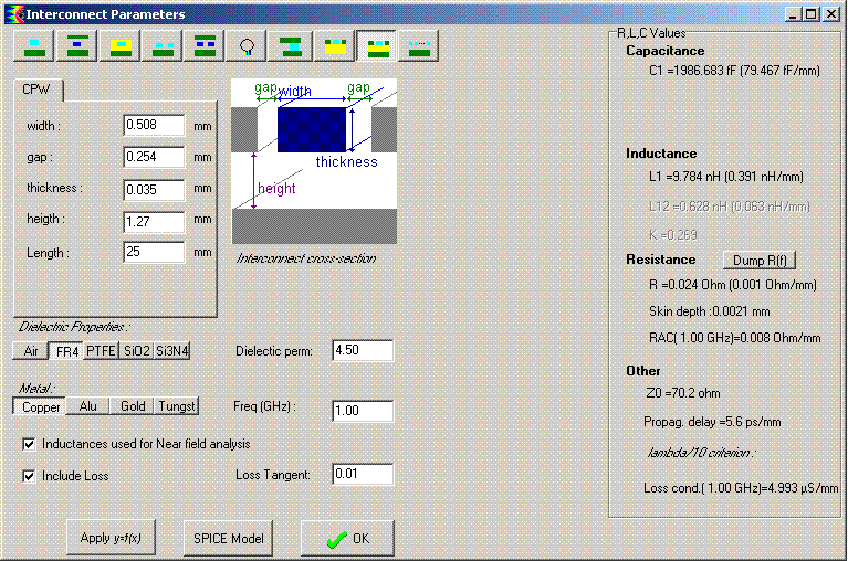
Automatic generation of transmission
line models
The IC-EMC tool "Interconnect Parameters" provides a set of analytical
formulas to extract electrical parameters of different kind of transmission
lines and interconnects (microstrip line, stripline, coplanar waveguide, parallel
lines, vias...). Electrical models based on quasistatic approximations can
be automatically generated for different types of analysis (impedance, S parameter,
transient, crosstalk, near field radiation).
[Top]
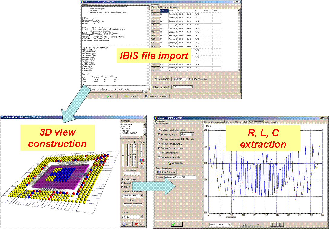
3D Package model extraction from
IBIS file
IBIS is a standardized format for analog interfaces of digital I/O buffers
modeling, which provides a right balance between comprehensive detail of the
IC and a sufficient accuracy for signal integrity simulation. IBIS is compenent-centric
i.e. it describes all pins of the physical component (pin-out, package, models).
A set of "hidden" keywords are added as comments in the IBIS file to describe the
IC package. From these keywords, the IC-EMC 3D
Package Viewer is able to build the 3D aspect of the package in order to locate
the placement of I/Os, especially power supply/groundpins. Coupled with the
tool Advanced SPICE and IBIS, R, L, C parasitic of package pins can be evaluated
rapidly based on closed-form analytical expressions.
[Top]
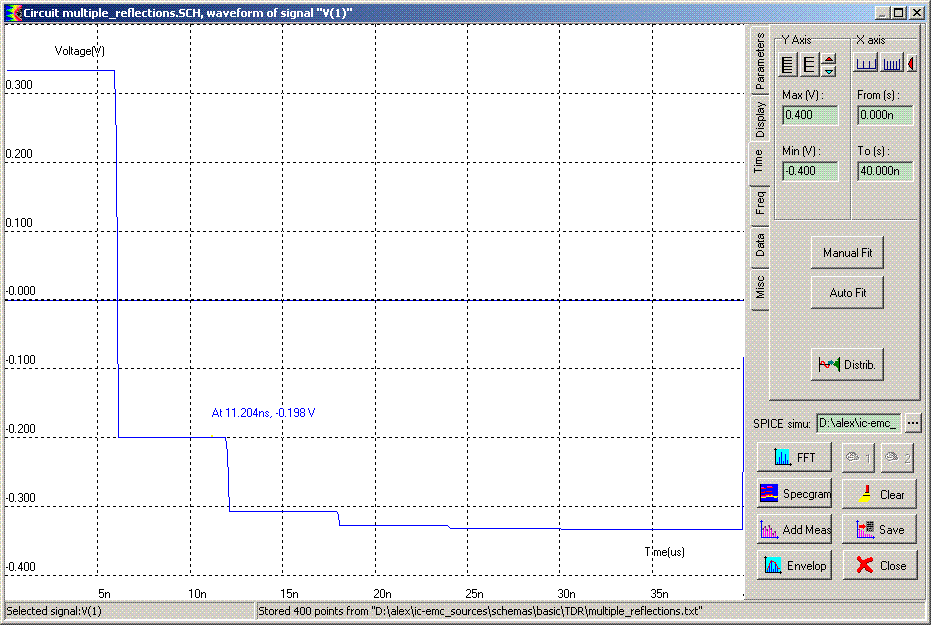
Time domain reflectometry
Signal integrity issues are related to impedance discontinuity in interconnects.
Time Domain Reflectometry is a valuable equipment used to locate impedance
impedance discontinuities and determine the nature of these discontinuities.
IC-EMC proposes a new symbol for TDR simulation in the palette symbol. Voltage
waveform, forward voltage, reflected voltage, impedance, reflection coefficient
profiles vs time can be simulated with this symbol. The figure below presents
an example of simulation of multiple reflections with the TDR symbol.
[Top]
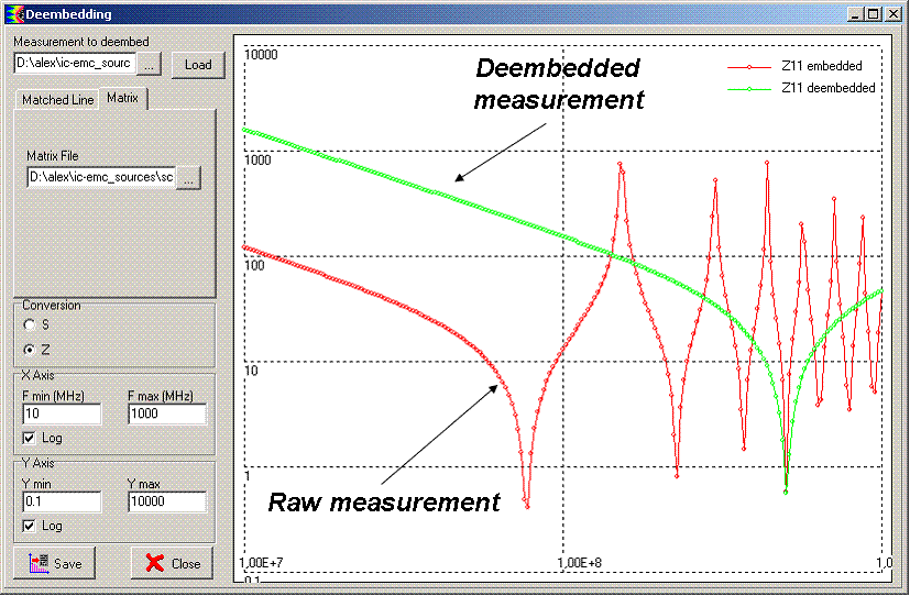
S parameter deembedding
Extracting the electrical model of a device from S parameter measurement
is often a complex operation due to the parasitic effects of the needed attachments
for connection of the device to the vector network analyzer, which should
be removed. The operation of deembedding allows to remove mathematically the
attachment from the measurements. IC-EMC proposes a tool which imports raw
S parameter measurement file in Touchstone file and deembeds the measurement.
The result, as shown on the figure below, corresponds to the measurement profile
that would be obtained if the measurement was done directly on the device
under test.
[Top]
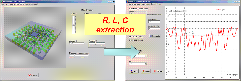
3D package model based on partial element
extraction
The accurate extraction of electrical parasitic elements associated to package
pins is a major issue to predict voltage bounce in IC. An accurate extraction
of package model requires a precise 3D geometrical model and the use of a
numerical method. The creation of geometrical model and numerical simulation
are time-consuming operations.
The tool Advanced Package Model proposes a
environment to simplify the construction of IC package and extract R, L, C
of each pins from partial elements computations based on quasi-static approximation.
Various types of package can be built (Quad Flat Package, Small Outline Package,
Ball Grid Array) from a set of geometrical information. The geometrical model
is then meshed and partial elements can be computed and displayed on a 2D
graph.
[Top]